Power Implications of Implementing Logic Using FPGA Embedded Memory Blocks
On-chip user memory has become a common resource on modern FPGAs.This memory comes in the form of configurable Embedded Memory Blocks (EMB). EMBs are very area efficient for implementing designs that require storage; However, for logic-intensive designs that do not require storage, the chip area devoted to EMBs become wasted. This need not be the case if the EMBs are configured as Read-Only-Memories (ROMs) and used to implement logic. Recall that a ROM is essentially a large Look-Up-Table (LUT), and LUTs are the traditional resource used to implement logic on an FPGA.
Several algorithms have been proposed that automatically map the logic portion of a design into ROMs and LUTs. Studies have shown that packing logic into ROMs can be very area efficient which can be beneficial for designs that are up against the logic capacity of the target FPGA. However these studies did not consider the impact on power and energy consumption.
Power has become a first-class concern among designers and is often the limiting factor in handheld battery-powered applications. In general, power affects packaging and cooling requirements which in turn affects production cost and device reliability.
In this article, we investigate the power implications of using EMBs to implement logic. We will first briefly review the EMB architecture and the basic ideas behind mapping logic to memories. Next we will look at how implementing logic in EMBs affect the overall FPGA energy consumption. Finally, we show that by combining multiple EMBs into larger logical memories, and mapping logic in such a way that some EMBs can be disabled on each access, we can reduce the power consumption of this technique.
FPGA Embedded Memory Block Features
Two features of FPGA embedded memory blocks are important for this article: configurable aspect ratio, and the ability to be configured as a RAM or ROM mode. To explain the configurable aspect ratio, we will use the M512 EMBs in the Altera Stratix devices as an example. These EMBs contain 512 memory bits but can be configured as one of the following aspect ratios: 512 1-bit words, 256 2-bit words, 128 4-bit words, 64 8-bit words, or 32 16-bit words. It is important to note that the shape of the physical memory does not change as the chip is configured (it is fixed when the FPGA is manufactured). The appearance of a con?gurable data width is obtained by using multiplexers and column enable signals to read and update only certain columns in each word.
Mapping Logic to ROMs
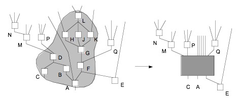
Several algorithms that map a design to ROMs and LUTs exist. We will briefly highlight the operations of the SMAP algorithm. Given a logic circuit that has already been mapped to LUTs (this is done by synthesis tools such as Altera Quartus Integrated Synthesis or Syplicity Synplify Pro), SMAP tries to pack as much logic into each available EMB as possible and leaves the rest of the logic in LUTs. The left side of Figure 1 shows a part of a design that has been mapped to a netlist of LUTs. The area shaded in grey has been identified by SMAP for mapping to a ROM. The right side of Figure 1 shows the design after the region has been replaced by a ROM. Inputs to the region of logic are connected to the address lines of the memory and outputs of the packed logic are connected to the memory outputs. The contents of the ROM are then programmed to store the truth-table of the outputs as a function of the inputs.
To identify the grey region, SMAP uses cut-based graph techniques. For each EMB that is available, SMAP will explore all parts of the design, and also try all possible aspect ratios of the EMB to find the mapping (grey region) that packs away the largest number of LUTs. To keep this article accessible, we omit the detailed workings of SMAP. However, more details can be obtained through the referenced journal paper at the end of the article.
Power Implications of Implementing Logic in EMBs
The main question that we will answer in this section is:
What is the overall impact on power dissipation when using EMBs to implement logic?
If large amounts of logic can be mapped into an EMB, not only are fewer LUTs required (which would save a small amount of power), but the interconnect between these LUTs are also not required (which would save a significant amount of power). On the other hand, EMBs themselves dissipate a significant amount of power.
To answer this question, we use an experimental methodology. We map a suite of benchmark circuits to an FPGA, and vary the number of EMBs available for implementing logic. Power data is gathered in two ways. The first method uses accepted academic FPGA CAD algorithms and power estimation models. In the second method, we mapped circuits using commercial CAD tools and performed current measurements on a 0.13um Altera Stratix (EP1S40) FPGA. The results are presented in units of energy per cycle to make them independent of operating frequency.
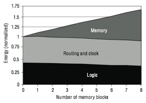
Figure 2 shows the averaged results using the academic power estimation models. The x-axis shows the number of 512-bit EMBs that were used to implement logic, and range from 0 (all logic implemented in LUTs) to 8. The vertical axis is energy normalized to the total energy when everything is implemented in LUTs. The bottom line corresponds to the energy consumed in the LUTs. As expected, this value decreases as the number of used EMBs increase. This is because more logic is packed away into ROMs as we use more EMBs, thus resulting in fewer LUTs in the final mapped circuit.
The second line indicates the sum of the logic energy and the energy consumed by the routing and the clock (so the area between the lower two lines represent the routing and clock energy). Again, as expected, more memory arrays means there are fewer LUTs, leading to fewer connections, and hence, lower routing energy. Finally, the top line is the overall energy; the di?erence between the top line and the middle line represents the energy consumed by the EMBs. As the graph shows, overall, mapping logic to EMBs does not reduce energy consumption. In fact, the energy increases signi?cantly as more memory arrays are used. This suggests that the extra power dissipated during a read access of the memory is larger than the power dissipated if the corresponding circuitry is implemented using lookup-tables.
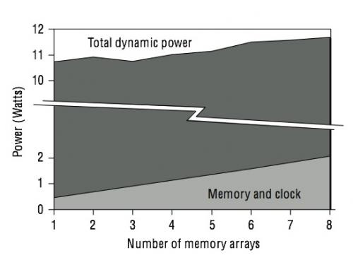
Figure 3 confirms these findings through current measurements on a real Altera Stratix device. This figure shows the results when only the M512 EMBs of the FPGA are used. The bottom line represents the power dissipated in the memories and clock network. The upper line presents the total power dissipated in the FPGA. In both cases, the static power was subtracted.
Power-Efficient Method For Mapping Logic to EMBs
The previous section showed that implementing logic in memory results in a severe power penalty. Yet, the significant area efficiency of the technique may motivate designers to implement logic in EMBs anyway, especially if the design is up against the capacity limits of the target FPGA. In this case, it is important to map logic to memories in as power-efficient a manner as possible. In this section, we describe one such method which applies a known power-optimization technique for RAM-mapping found in Altera Quartus II CAD suite.
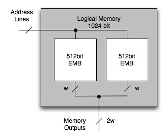
The key to this idea is to first combine two or more EMBs into larger logical EMBs, and then map logic to these logical memories. However, we must combine EMBs in a specific way to make it power efficient. Figure 4 shows how two 512-bit EMBs can be combined to form a larger logical EMB with 1024 bits. The configurable aspect ratio for this logical block can be one of 512 2-bit words, 256 4-bit words, 128 8-bit words, 64 16-bit words, 32 32-bit words. In this configuration, each EMB implements half of the output bits. However, in each access to this logical EMB, both physical EMBs are active and dissipate power.
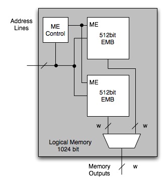
Figure 5 shows a more power efficient way of combining two EMBs. This logical EMB also has 1024 bits but has a different set of configurable aspect ratios: 1024 1-bit words, 512 2-bit words, 256 4-bit words, 128 8-bit words, and 64 16-bit words. In this configuration, each physical EMB implements all of the output bits. However, one of the EMBs can be disabled to conserve power in each access. The trade-off is that extra logic must be used to implement the memory enable control logic and output multiplexors and this reduces area efficiency. In general, more than two EMBs can be joined to form logical EMBs.
When multiple EMBs are available for implementing logic, it is thus more power-efficient to first combine them into larger logical EMBs. However, due to the extra support logic required, the area efficiency of mapping logic to memories is reduced.
Summary
In this article, we showned that implementing logic in FPGA embedded memory blocks leads to an increase in power dissipation of the resulting circuit despite being very area efficient. If designers wish to implement logic in EMBs, it is important to carefully tradeo? the power penalties with the potential increase in density. We also discussed a technique that can achieve power savings by combining multiple physical memories into larger logical memories and mapping logic to the logical memories. To form the logical memories from the physical memories, we used a power-e?cient arrangement that allows one or more of the physical memories to be disabled in each cycle. However, using this technique requires additional support logic implemented in LUTs.
For the full details of our experimental findings, methodologies and algorithms, please refer to the journal paper describing this work in the related links section below.
For further information, contact Scott Chin, University of British Columbia, [email protected]
About Author


![]()
![]()

Check out FPGA related videos

Find Us On Facebook
FPGA Central is a website bringing the FPGA (Field Programable Gate Array), CPLD , PLD, VLSI community together at one central location. Some Keywords: FGPA, FPGA, EDA Tools, FPGA Design, Central, Programmable logic, LUT, VLSI, SoC, Journal
Privacy Policy || Terms of Use
 |
 |
Comments
December 25, 2008 - 12:12pm
C to Verilog
Hi,
I don't know if you know about this but C To Verilog is a website which compiles regular C code into Verilog. There is a free on-line service on the webpage. Maybe you can review it and write a post about it.
Nadav